

Wafer OCD Measurement System Market to Reach USD 1.81 Billion by 2034 Driven by Advanced Node Fabrication and AI Chip Production
Wafer OCD Measurement System Market to Reach USD 1.81 Billion by 2034 Driven by Advanced Node Fabrication and AI Chip Production
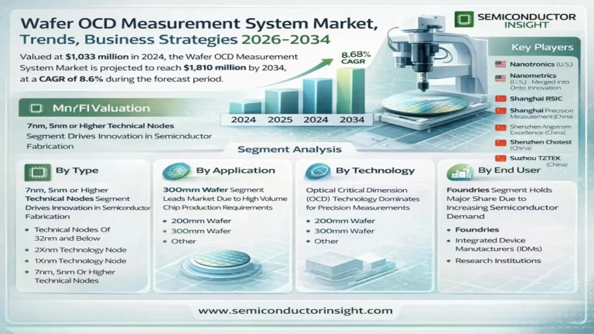
Global Wafer OCD Measurement System Market was valued at USD 1,033 million in 2026 and is projected to reach USD 1,810 million by 2034, expanding at a CAGR of 8.6% during the forecast period. Market growth is being fueled by rapid advances in semiconductor process nodes.
Wafer OCD (Optical Critical Dimension) measurement systems are precision metrology instruments used in semiconductor manufacturing to measure and analyze nanoscale features during wafer processing. These systems apply advanced optical and scatterometry-based techniques to evaluate parameters such as line width, pattern profile, and thin-film thickness, ensuring process control and yield optimization.
For a detailed analysis of market drivers, restraints, opportunities, and the competitive strategies of key players, access the complete report.
https://semiconductorinsight.com/report/wafer-ocd-measurement-system-market-size/
Market Overview
The market is expanding alongside global semiconductor capacity additions and node shrink roadmaps. With dozens of new fabs planned or under construction through the next decade, demand for advanced in-line metrology and process control tools is rising steadily. OCD measurement systems are now deeply integrated into advanced logic and memory manufacturing flows, supporting tighter tolerances and complex multi-pattern structures.
Advanced Node Development
Migration to 7nm, 5nm, and more advanced nodes requires ultra-precise dimensional measurement and profile control. OCD systems provide non-destructive, high-throughput metrology needed for these process generations.
Skilled Metrology Workforce Shortage
Operation and calibration of advanced OCD systems require deep expertise in optics, materials science, and semiconductor physics. A shortage of trained professionals is creating deployment and scaling bottlenecks across fabs.
Accuracy Limits at Sub-5nm Dimensions
At extremely small geometries, measurement reliability faces physical and modeling limits. Quantum and material interaction effects introduce variability, increasing recalibration needs and operational complexity.
Competitive Landscape
Mergers and portfolio consolidations have also shaped the landscape, strengthening end-to-end process control offerings.
Key Wafer OCD Measurement System Manufacturers
- KLA Corporation
- Onto Innovation
- NOVA
- Nanotronics
- Nanometrics (now part of Onto Innovation)
- Shanghai RSIC
- Shanghai Precision Measurement
- Shenzhen Angstrom Excellence
- Shenzhen Chotest
- Suzhou TZTEK Technology
Segment Analysis
By Technology Node
- Technical Nodes of 32nm and Below
- 2Xnm Technology Node
- 1Xnm Technology Node
- 7nm, 5nm or Higher Technical Nodes
By Wafer Size
- 200mm Wafer
- 300mm Wafer
- Others
By Technology
- Optical Critical Dimension (OCD)
- Scatterometry
- Spectroscopic Ellipsometry
- Others
By End User
- Foundries
- Integrated Device Manufacturers (IDMs)
- Research Institutions
Regional Insights
North America
North America remains a major market driven by leading chip designers and manufacturers, strong R&D activity, and government semiconductor incentives. Advanced node and AI chip programs are key demand sources.
Europe
Europe shows steady adoption supported by automotive, industrial, and specialty semiconductor production. Regional chip initiatives are expected to gradually strengthen metrology demand.
Asia-Pacific
Asia-Pacific dominates global demand with over 70% share, led by China, Taiwan, South Korea, and Japan. Concentration of leading fabs and OSAT players makes the region the primary growth engine for OCD systems.
Report Scope
The report provides a comprehensive analysis of the Global Wafer OCD Measurement System Market for the forecast period 2026–2034, including market size and growth forecasts, segmentation by node, wafer size, technology, and end user, regional demand analysis, competitive benchmarking of leading suppliers, and detailed evaluation of technology and process control trends shaping next-generation semiconductor manufacturing.
Download sample report:
https://semiconductorinsight.com/download-sample-report/?product_id=103156
About Semiconductor Insight —About Semiconductor Insight
Semiconductor Insight is a global intelligence platform delivering data-driven market insights, technology analysis, and competitive intelligence across the semiconductor and advanced electronics ecosystem. Our reports support OEMs, investors, policymakers, and industry leaders in identifying high-growth markets and strategic opportunities shaping the future of electronics.
🌐 https://semiconductorinsight.com/
🔗 LinkedIn: Follow Us
📞 International Support: +91 8087 99 2013