

Top 10 Leading Players in the Sputtering Equipment for Semiconductors Market Projected to Achieve a CAGR of 7.0% by 2034
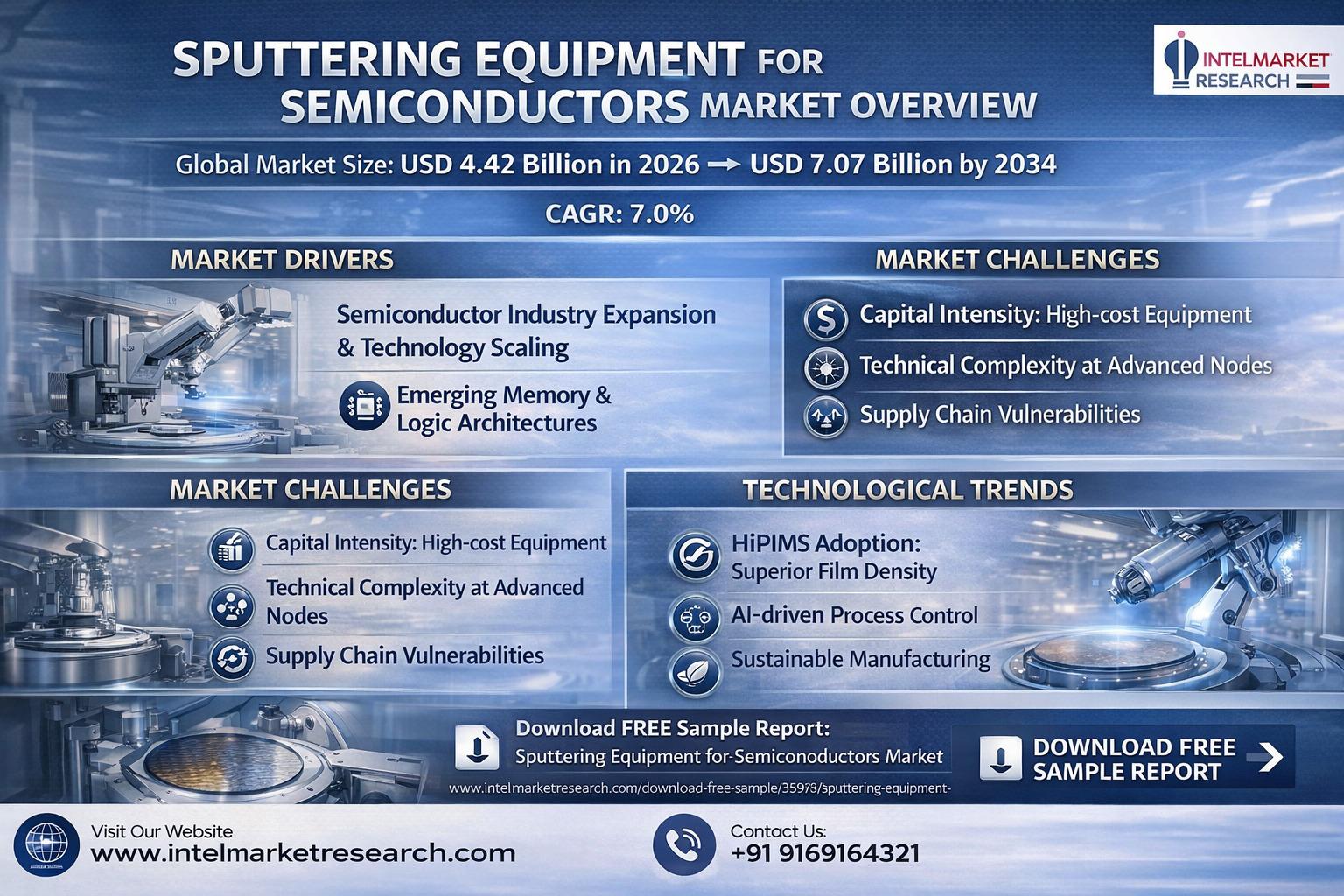
According to a new report from Intel Market Research, Global sputtering equipment for semiconductors market was valued at USD 4.42 billion in 2025 and is projected to reach USD 7.07 billion by 2034, growing at a steady CAGR of 7.0% during the forecast period (2026–2034). This growth trajectory reflects the expanding semiconductor industry's demand for advanced deposition technologies and the increasing complexity of chip manufacturing processes.
📥 Download FREE Sample Report: Sputtering Equipment for Semiconductors Market - View in Detailed Research Report
📥 Download FREE Sample Report: https://www.intelmarketresearch.com/download-free-sample/35970/sputtering-equipment-for-semiconductors-market
What is Sputtering Equipment?
Sputtering equipment represents the backbone of physical vapor deposition (PVD) technology essential for semiconductor manufacturing. Through a precision-controlled process where high-energy ions bombard target materials, atoms are ejected and deposited onto wafers with atomic-level accuracy. This technology enables the creation of critical conductive layers, barrier films, and specialized coatings that form the nervous system of modern chips.
The semiconductor industry's insatiable appetite for more powerful, energy-efficient chips continues driving innovation in sputtering systems. From cutting-edge 3D NAND memory stacks to advanced logic devices requiring angstrom-level precision, modern sputtering solutions must meet increasingly stringent requirements for film quality, uniformity, and throughput.
This report delivers a 360-degree view of the sputtering equipment landscape, encompassing everything from technological breakthroughs to regional market dynamics. It provides executives and engineers alike with actionable intelligence to navigate this complex, capital-intensive sector.
Key Market Drivers
1. Semiconductor Industry Expansion and Technology Scaling
The global semiconductor shortage underscored the critical need for expanded production capacity. Foundries and IDMs are investing heavily in new facilities, with TSMC alone budgeting $36 billion for capital expenditures in 2024. Each new fab requires dozens of sputtering tools, particularly for advanced nodes where deposition processes multiply. The transition to GAA (Gate-All-Around) transistors at 3nm and below creates additional demand for atomic-layer precise deposition capabilities.
2. Emerging Memory and Logic Architectures
Innovations in semiconductor design are reshaping deposition requirements:
-
3D NAND - With stacks exceeding 200 layers, the need for high-aspect-ratio step coverage has never been greater
-
MRAM/ReRAM - Next-generation memories require specialized magnetic and oxide materials with exceptional uniformity
-
Chiplet Integration - Advanced packaging demands precise deposition for interconnects and thermal management
These architectural shifts are pushing sputtering technology beyond traditional aluminum and copper interconnects into new material frontiers.
Market Challenges
-
Capital Intensity - A single 300mm sputtering tool now costs $3-5 million, creating high barriers to entry for smaller chipmakers
-
Technical Complexity - Maintaining yield at 3nm nodes requires plasma stability measurements every few milliseconds
-
Supply Chain Vulnerabilities - Critical components like ceramic heaters and RF generators face extended lead times
While these challenges are substantial, they also create opportunities for equipment vendors who can deliver solutions combining precision, reliability, and total cost of ownership advantages.
Technological Trends Shaping the Future
The industry is witnessing several transformative developments:
-
HiPIMS Adoption - High-power impulse magnetron sputtering enables superior film density for critical barrier layers
-
AI-driven Process Control - Machine learning algorithms optimize deposition parameters in real-time
-
Sustainable Manufacturing - New systems reduce argon consumption and power usage per wafer
These innovations help chipmakers balance the competing demands of performance, cost, and sustainability in an increasingly complex technical landscape.
Regional Market Dynamics
Asia-Pacific Dominance
Accounting for over 60% of global semiconductor production, Asia remains the epicenter of sputtering equipment demand. China's aggressive fab expansion, despite trade restrictions, continues to drive significant equipment purchases. Meanwhile, established hubs like Taiwan and Korea are upgrading existing facilities for next-generation nodes.
North American Resurgence
The U.S. CHIPS Act has sparked over $200 billion in announced investments, with Intel, TSMC, and Samsung all building advanced fabs in Arizona. This surge creates new opportunities for equipment suppliers with strong domestic support networks.
European Specialization
While trailing in volume, Europe maintains leadership in specialized applications like power semiconductors and MEMS sensors, requiring customized sputtering solutions.
📥 Download FREE Sample Report: Sputtering Equipment for Semiconductors Market - View in Detailed Research Report
Competitive Landscape
The sputtering equipment sector remains highly concentrated, with the top three players controlling over 50% market share. Applied Materials maintains technology leadership through continuous R&D investments, while Tokyo Electron leverages its strong foundry relationships. Challengers like ULVAC and Canon Anelva compete through specialization in emerging applications.
Key differentiators include:
-
Advanced process control capabilities
-
Service network responsiveness
-
Energy efficiency metrics
-
Total cost of ownership
As the industry moves toward more customized solutions, the ability to co-develop processes with leading chipmakers becomes increasingly crucial.
Market Segmentation
By Technology Type
-
Magnetron Sputtering
-
Ion Beam Sputtering
-
Reactive Sputtering
-
HiPIMS
By Application
-
Logic Devices
-
Memory (DRAM/NAND)
-
Advanced Packaging
-
Power Semiconductors
By Wafer Size
-
200mm (Legacy)
-
300mm (Mainstream)
-
450mm (Emerging)
📘 Get Full Report Here: Sputtering Equipment for Semiconductors Market - View Detailed Research Report
About Intel Market Research
Intel Market Research is a leading provider of strategic intelligence, offering actionable insights in semiconductors, advanced manufacturing, and industrial technologies. Our research capabilities include:
-
Real-time competitive benchmarking
-
Global technology adoption tracking
-
Comprehensive supply chain analysis
-
Over 500+ technical market reports annually
Trusted by Fortune 500 companies worldwide, our insights empower decision-makers to navigate complex technology transitions with confidence.
🌐 Website: https://www.intelmarketresearch.com
📞 Asia-Pacific: +91 9169164321
🔗 LinkedIn: Follow Us